

Decoding Science 021: Boron Toughens Alloys at 2,400 °C, and a Mamyshev Oscillator Shrinks a Laser onto a Chip


Welcome to Decoding Science: every other week our writing collective highlight notable news—from the latest scientific papers to the latest funding rounds in AI for Science —and everything in between. All in one place.


What we read
Ductile alloys offering 100 MPa tensile strength at 2,400 °C [Xue et al., Nature, June 2026]
Materials and extreme environments usually do not interact favorably. High temperature applications are particularly challenging as the thermal energy facilitates unfavorable microstructure evolution and subsequent reductions in mechanical strength at just 60% of the melting temperature in even the most advanced of high-temperature alloys. However, as demand grows for space travel (particularly with regards to re-entry) and the development of next gen nuclear reactors and hypersonic planes accelerates, the need for materials which can withstand temperatures of greater than 2000 °C while maintaining structural and geometric integrity grows. Existing materials (ceramics, intermetallics, and refractory materials) struggle to meet these criteria while also suffering from low ductility at room temperature which greatly limits the complexity of the parts that can be manufactured. In their recent paper, Xue et al. describe a boron-stabilized HfO2-strengthened Ta-based alloy which meets these needs, having a tensile yield strength of 200 MPa at 2000 °C and 100 MPa at 2400 °C with an elongation-to-failure of about 35%.
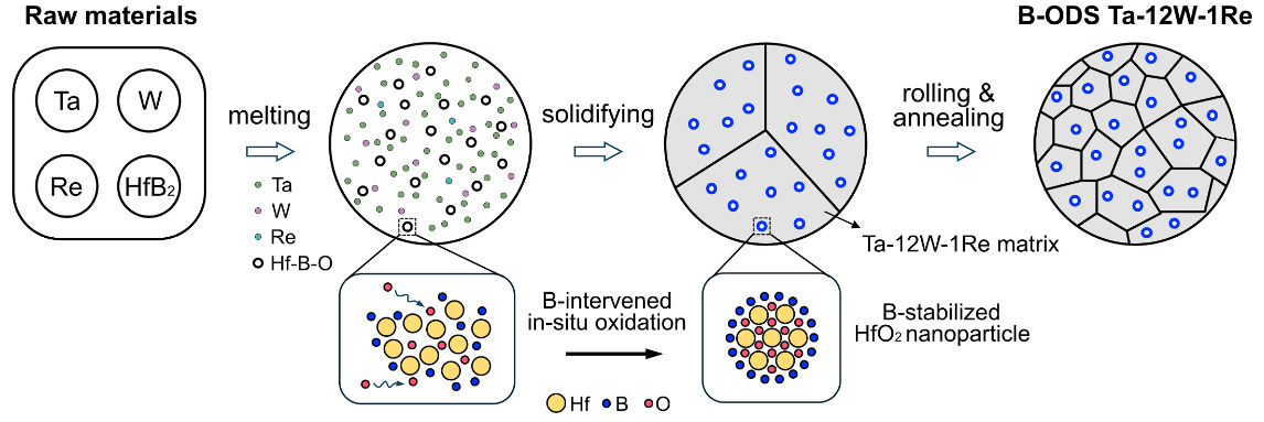
The alloy is made via oxide-dispersion strengthening (ODS), in which 0.4 wt% HfB2 is added to body-centered-cubic Ta-12W-1R. As the mixture is melted, the oxide impurities present in the refractory matrix react with the HfB2 particles, displacing the B to form highly stable HfO2 particles. Using three-dimensional atom probe tomography (3D-APT), the authors found that the liberated B aggregates in the interface between the nanoparticle and bulk matrix. This accumulation creates a barrier which prevents the growth of the oxide nanoparticles via diffusion at higher temperatures, a process which can significantly degrade performance. TEM imaging also validated that the oxide nanoparticles formed homogeneously throughout the material—rather than preferentially at the grain boundaries—due to boron accumulation which blocked grain boundary oxidation sites.
When analyzing the mechanism underpinning the increase in elongation, the authors found that the substantial stability of the oxides promotes hardening of the bulk material via the Orowan mechanism, helping to trap the dislocations in loops around the particles upon elongation. Additionally, as the material experiences greater strain, deformations accumulate around the nanoparticles, but the oxides at these sites are able to partially alleviate the localized strain by plastically deforming themselves, improving ductility by preventing brittle fracture. Only about 20% of the oxides were observed to do so at 35% elongation.
The boron ODS process can also be applied to other materials, as demonstrated with another Ta-based alloy (Ta-10W-3V) and a Nb-W alloy. Both demonstrated improved elongation-at-failure, with the Ta alloy increasing from 30% to 40% while the Nb-W alloy jumped from 3% to 18% while retaining high tensile strengths. These examples demonstrate how the ODS process described in the paper to increase ductility and thermal stability positions itself to be a promising platform for the discovery of functional, high temperature materials.
High-pulse-energy integrated mode-locked laser using a Mamyshev oscillator [Qiu et al., Nature, June 2026]
The mode-locked laser is behind how every optical atomic clock, femtosecond eye surgery, and frequency comb (to name a few) are able to operate. Yet these sci-fi like technology of ultrafast science still rely on bulky benchtop or fibre systems. Scientists have spent decades trying to shrink them onto photonic chips, but every attempt so far to miniaturize the process of making short bursts of light has stalled at a few picojoules of pulse energy, which is too feeble to drive the nonlinear optics that make ultrafast lasers useful in the first place.
This work by Qiu et al. at EPFL closes that gap by two orders of magnitude using a Mamyshev oscillator. The laser is a 42-cm light-guiding channel coiled onto a fingernail-sized chip, with a color filter at each end — and because the two filters pass different colors, dim steady light can never make it through both, while intense pulses stretch their own color range wide enough to slip past. This filtering trick, built on an erbium-doped silicon nitride waveguide between two spectrally offset Bragg gratings, replaces the fragile saturable absorber that conventional mode-locked lasers depend on. There’s a catch to putting a laser on a chip like this: the tightly confined waveguides are a thousand times more nonlinear than fibre, and pulses circulating in them accumulate distortions that destroy conventional mode-locked lasers. The Mamyshev oscillator tolerates enormous distortions — phase shifts up to 60π — which is why it works here where other designs fail. The result delivers 1.04-nJ pulses, a hundredfold jump over previous chip lasers, with a 64-nm spectrum spanning the telecom band, compression to 147 fs, comb lines pure enough (31.4 kHz) for precision metrology, and ten straight hours of operation. And that pulse energy pays off immediately: with no amplification at all, the raw output directly powered a terahertz spectrometer sensitive enough to fingerprint lactose against flour by their absorption spectra.
With over 300 lasers per wafer, portable THz inspection and chip-scale frequency metrology may now have a possible route to reaching commercialization. But keep in mind that this is a demonstrative laser, not a complete system: the pulse compression still runs through 10 m of external fibre, and the supercontinuum (light stretched across a huge swath of spectrum, the prerequisite for self-referenced frequency combs and optical clocks) lives on a second chip. Integrating dispersion-engineered compression and octave-spanning broadening on the same die, which they plan to do next, is what would turn this milestone into the self-referenced comb on a chip the field has been chasing.
Other links:
EinsteinArena turns a crowd of AI agents loose on open math problems, and they already beat 12 human and machine records including the kissing number bound in dimension 11
Notable Deals
Atinary raised fresh capital for its cloud lab that runs chemistry on its own, producing about a PhD worth of experimental data every week.
Meta unveiled Brain2Qwerty v2 , decoding typed sentences from brain scans at 61% word accuracy and no surgery needed.
Nvidia handed academic labs a standard humanoid robot kit at GTC Taipei.
Field Trip
Did we miss anything? Would you like to contribute to Decoding Science by writing a guest post? Drop us a note here or chat with us on X.
 | A guest post by
|